PCB fabrication and assembly address EMI and EMC issues
PCB fabrication and assembly play a crucial role in addressing electromagnetic interference (EMI) and electromagnetic compatibility (EMC) issues in electronic devices. As electronic circuits become increasingly compact and operate at higher speeds, the potential for EMI—unwanted electromagnetic radiation—and the need for EMC—ensuring a device operates as intended without causing or being affected by interference—becomes more significant. Proper design and manufacturing techniques are essential to mitigate these issues, ensuring that the final product is reliable, efficient, and compliant with industry standards.
One of the key ways that PCB fabrication and assembly address EMI and EMC issues is through careful circuit layout and design. In PCB design, the trace routing, component placement, and layer stack-up must be optimized to minimize EMI and enhance the PCB’s overall performance. For instance, by keeping high-speed signal traces as short and direct as possible, designers can reduce the opportunity for signal interference and radiation. Additionally, the layout should focus on maintaining adequate spacing between high-frequency components and sensitive analog circuits to minimize cross-talk and unintended coupling of signals. In high-frequency designs, designers may use specific routing techniques, such as differential pairs or controlled impedance traces, to ensure that signals remain balanced and minimize noise susceptibility.
Another important consideration in pcb fabrication and assembly is the use of ground planes and power planes. A solid ground plane helps to create a reference point for the electrical signals and reduces the potential for EMI by providing a low-resistance path for return currents. In multi-layer PCBs, the use of separate ground and power planes also helps isolate noise-sensitive components from noisy signals, preventing cross-talk and interference. Ensuring a continuous and well-connected ground plane throughout the PCB is vital for maintaining EMC performance, as it provides an effective shielding mechanism to contain electromagnetic emissions.
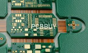
How does PCB fabrication and assembly address EMI and EMC issues?
In addition to optimizing the design, PCB fabrication and assembly also incorporate physical shielding techniques to further reduce EMI. This can be achieved by using materials that have high conductivity or magnetic permeability to create protective barriers around sensitive areas of the PCB. These shields act as Faraday cages, confining electromagnetic radiation within the PCB and preventing it from escaping or entering sensitive components. During assembly, components such as capacitors, inductors, and ferrite beads may also be added to filter out high-frequency noise and suppress EMI. These components help to mitigate the effects of electromagnetic interference by either absorbing or redirecting unwanted signals, ensuring that the device operates within acceptable EMC limits.
In some cases, PCB fabrication and assembly address EMI and EMC by incorporating surface treatments or coatings. For example, applying conductive coatings to the PCB’s surface can further reduce the potential for EMI by creating a conductive layer that shields the board from external interference. Solder masks, which are used to protect the PCB’s copper traces, can also contribute to reducing electromagnetic emissions by covering unwanted conductive areas and preventing unintentional short circuits that could lead to interference.
Proper component selection during assembly is another critical factor in addressing EMI and EMC issues. For example, components like low-noise transistors, specialized connectors, and properly shielded components are often selected for designs where minimizing EMI is a top priority. Additionally, PCB assembly processes can be optimized to ensure that components are placed in such a way that minimizes the creation of electromagnetic fields or current loops that might lead to interference. For instance, placing decoupling capacitors close to power pins of ICs can help stabilize voltage levels and reduce the risk of power-related EMI.
Furthermore, testing and validation during the PCB fabrication and assembly process are crucial for ensuring that EMI and EMC issues are adequately addressed. After assembly, the PCB is subjected to various testing methods, such as radiated and conducted EMI testing, to ensure that the device complies with the required standards set by regulatory bodies like the Federal Communications Commission (FCC) or the European Union’s EMC directive. If the device fails these tests, further design iterations or additional shielding techniques may be implemented to reduce emissions or improve immunity.
In conclusion, PCB fabrication and assembly address EMI and EMC issues through a combination of careful design, physical shielding, component selection, and testing. By optimizing layout, using appropriate materials, and incorporating passive components that suppress noise, manufacturers can minimize electromagnetic interference and enhance the electromagnetic compatibility of the device. These efforts are essential for ensuring that electronic devices operate reliably without negatively impacting or being affected by other electronic systems, meeting regulatory requirements and delivering high-performance, interference-free products.